NCERT Solutions for Class 12 Physics Chapter 14 - Semiconductor Electronics Materials Devices And Simple Circuit
Upcoming Event
CBSE Class 12th Exam Date:17 Feb' 26 - 17 Feb' 26
From mobile phones to PCS, LEDS to solar cells — semiconductors are the fundamental building materials of contemporary electronic devices. The knowledge of their operation is necessary for every student who is attempting to excel at physics and has a career linked with technology.
This Story also Contains
- NCERT Solutions for Class 12 Physics Chapter 14: Download PDF
- Class 12 Physics Chapter 14: Exercise Solution
- Semiconductor Electronics: Materials, Devices and Simple Circuits: Additional Questions
- Class 11 physics NCERT Chapter 12: Higher Order Thinking Skills (HOTS) Questions
- Semiconductor Electronics: Materials, Devices and Simple Circuits Class 12 Chapter 14: Topics
- Semiconductor Electronics: Materials, Devices and Simple Circuits Class 12 Chapter 14: Notes
- Approach to Solve Questions of Semiconductor Electronics: Materials, Devices and Simple Circuits
- What Extra Should Students Study Beyond NCERT for JEE/NEET?
- NCERT solutions for class 12 physics chapter-wise
Chapter 14 – Semiconductor Electronics: Materials, Devices and Simple Circuits is a crucial chapter in NCERT Class 12 Physics, especially for those students who are preparing for board-level exams or competitive exams like the JEE and NEET. In order to have a better grasp of the topic, it is highly recommended to study the NCERT Solutions of the chapter under study.
These responses are the correct and proper answers to each question that are located in the NCERT Class 12 Physics book. Authored by subject experts, the content is written in an understandable form that is apt for students. The descriptions are meant to demystify complex concepts, such as semiconductor materials, p-n junction diodes, rectifiers, transistors, and applications. For their optimal achievement, the students must supplement their textbook study with these NCERT solutions for Class 12 and other study materials for better understanding and effective revision.
Also read :
NCERT Solutions for Class 12 Physics Chapter 14: Download PDF
Access the PDF version of Class 12 Semiconductor Electronics: Materials, Devices and Simple Circuit NCERT Solutions by clicking on the download button. Using the PDF version, you can view the solutions offline and revise the essential exercise questions at your own convenience.
Class 12 Physics Chapter 14: Exercise Solution
Q. 14.1 In an n-type silicon, which of the following statement is true:
(a) Electrons are majority carriers and trivalent atoms are the dopants.
(b) Electrons are minority carriers and pentavalent atoms are the dopants.
(c) Holes are minority carriers and pentavalent atoms are the dopants.
(d) Holes are majority carriers and trivalent atoms are the dopants.
Answer:
An N-type semiconductor has electron as majority carriers and holes as minority carriers. It is formed when we dope pentavalent impurity in Silicon atom. Some pentavalent dopants are phosphorus, arsenic, and bismuth.
Hence, the correct option is C.
Q. 14.2 Which of the statements given in Exercise 14.1 is true for p-type semiconductors.
(a) Electrons are majority carriers and trivalent atoms are the dopants.
(b) Electrons are minority carriers and pentavalent atoms are the dopants.
(c) Holes are minority carriers and pentavalent atoms are the dopants.
(d) Holes are majority carriers and trivalent atoms are the dopants
Answer:
In a p-type semiconductor, holes are the majority carrier and electrons are the minority carrier. It is formed when a trivalent atom-like aluminium is doped in a silicon atom. Hence correct option for p-type conductor would be (d).
(a) $(E_{g})_{Si} < (E_{g})_{Ge}< (E_{g})_{C}$
(b) $(E_{g})_{C} < (E_{g})_{Ge}> (E_{g})_{Si}$
(c) $(E_{g})_{C} > (E_{g})_{Si}> (E_{g})_{Ge}$
(d) $(E_{g})_{C} = (E_{g})_{Si}= (E_{g})_{Ge}$
Answer:
Since carbon is a non-metal, its energy band gap would be highest and energy band gap of Ge would be least as it is a metalloid.
$(E_{g})_{C} > (E_{g})_{Si}> (E_{g})_{Ge}$
Hence correct option would be (c)
Q14.4 In an unbiased p-n junction, holes diffuse from the p-region to n-region beca
(a) free electrons in the n-region attract them
(b) they move across the junction by the potential difference.
(c) hole concentration in p-region is more as compared to n-region.
d) All the above
Answer:
Charge flows from higher concentration to the lower concentration in a junction. In this case, holes are diffusing from the p-region to n-region and hence the concentration of hole is greater in p region.
and hence correct option would be (c)
Q. 14.5 When a forward bias is applied to a p-n junction, it
(a) raises the potential barrier
(b) reduces the majority carrier current to zero.
(c) lowers the potential barrier.
(d) none of the above.
Answer:
When a p-n junction is forward biased, the negative voltage repels the electron toward junction and give them the energy to cross the junction and combine with the hole which is also being pushed by a positive voltage. This leads to a reduction in the depletion layer which means a reduction in potential barrier across the junction.
Hence correct option would be (c)
Answer:
As we know :
output frequency for half-wave rectifier = input frequency, and hence output frequency in half-wave rectifier will be 50Hz.
also, output frequency for full-wave rectifier = 2*(input frequency) and Hence output frequency in full-wave rectifier will be 2*50 = 100 Hz.
Semiconductor Electronics: Materials, Devices and Simple Circuits: Additional Questions
Answer:
Given
the energy band gap of photodiode is 2.8eV.
wavelength = $\lambda$ = 6000nm = $6000*10^{-9}$
The energy of signal will be $\frac{hc}{\lambda }$
where c is speed of light(300000000m/s) , h is planks constant ( = $6.626 * 10^{-34}Js$ )
putting the corresponding value
The energy of signal = $\frac{(6.626 * 10^{-34} * 3*10^8)}{6000*10^{-9}}$
= $3.313*10^{-20}J$
= $0.207eV (since 1.6*10^{-20}= 1eV)$
The energy of the signal is 0.207eV which is less than 2.8eV ( the energy and gap of photodiode). Hence signal can not be detected by the photodiode.
Answer:
Given:
number of Silicon atoms per $m^{3}$ = $5\times 10^{28}.$
number of Arsenic atoms per $m^{3}$ = $5\times 10^{22}.$
number of Indium atoms per $m^{3}$ = $5\times 10^{20}$
number of thermally generated electrons $n_{i}=1.5\times 10^{16}\; m^{-3}.$
Now,
Number of electrons
$n_e =$ $5 * 10 ^{22}-1.5*10^{16}$ = $4.99*10^{22}(approx)$
number of holes is $n_h$
in thermal equilibrium
$n_h*n_e=n_i^2$
$n_h=n_i^2/n_e$
$n_h= (1.5*10^{16})^2/4.99*10^{22}$
$n_h= 4.51 * 10^9$
Now, since the number of electrons is higher than number of holes, it is an n-type semiconductor.
$n_{i}=n_{0}\; exp\left [ -\frac{E_{g}}{2K_{B}T} \right ]$
Where, $n_{0}$ is constant.
Answer:
Energy gap of given intrinsic semiconductor = E g = 1.2eV
temperature dependence of intrinsic carrier concentration $n_{i}$ is given by
$n_{i}=n_{0}\; exp\left [ -\frac{E_{g}}{2K_{B}T} \right ]$
Where is constant, $K_B$ is Boltzmann constant = $8.862 * 10^{-5}eV/K$ ,
T is temperature
Initial temperature = T1 = 300K
the intrinsic carrier concentration at this temperature :
$n_{i1} = n_0exp[\frac{-E_g}{2K_B*300}]$
Final temperature = T2 = 600K
the intrinsic carrier concentration at this temperature :
$n_{i2} = n_0exp[\frac{-E_g}{2K_B*600}]$
the ratio between the conductivities at 300K and at 600K is equal to the ratio of their intrinsic carrier concentration at these temperatures
$\frac{n_{i2}}{n_{i2}} = \frac{n_0exp[\frac{-E_g}{2K_B*600}]}{n_0exp[\frac{-E_g}{2K_B*300}]}$
$= exp\frac{E_g}{2K_B}[\frac{1}{300}-\frac{1}{600}]=exp[\frac{1.2}{2*8.62*10^{-5}}* \frac{2-1}{600}]$
$= exp[11.6] = 1.09 * 10^{5}$
Therefore the ratio between the conductivities is $1.09 * 10^{5}$ .
Q.4 In a p-n junction diode, the current I can be expressed as
$I=I_{0}\; [exp \frac{eV}{K_{B}T}-1 ]$
where $I_{0}$ is called the reverse saturation current, V is the voltage across the diode and is positive for forward bias and negative for reverse bias, and $I$ is the current through the diode, $k_{B}$ is the Boltzmann constant $(8.6\times 10^{-5}eV/K)$ and $T$ is the absolute temperature. If for a given diode $I_{0}=5\times 10^{-12}A$ and $T=300\; K,$ then
(a) What will be the forward current at a forward voltage of $0.6\; V\; ?$
Answer:
As we have
$I=I_{0}\; [exp \frac{eV}{K_{B}T}-1 ]$
Here, $I_{0}=5\times 10^{-12}A$ , $T=300\; K,$ and , $k_{B}$ = Boltzmann constant = $(8.6\times 10^{-5}eV/K)$ $=(1.376*10^{-23}J/K)$
When the forward voltage is 0.6V:
$I=5*10^{-12}\;[ exp \frac{1.6*10^{-19}*0.6}{1.376*10^{-23}*300}-1 ]=0.0625A$
Hence forward current is 0.0625A
Q.5 In a p-n junction diode, the current I can be expressed as
$I=I_{0}\; [exp \frac{eV}{K_{B}T}-1 ]$
where I0 is called the reverse saturation current, $V$ is the voltage across the diode and is positive for forward bias and negative for reverse bias, and $I$ is the current through the diode, $k_{B}$ is the Boltzmann constant $(8.6\times 10^{-5}\; eV/K)$ and $T$ is the absolute temperature. If for a given diode $I_{0}=5\times 10^{12}A$ and $T=300\; K,$ then
(b) What will be the increase in the current if the voltage across the diode is increased to $0.7 \; V?$
Answer:
As we have
$I=I_{0}\; [exp \frac{eV}{K_{B}T}-1 ]$
Here, $I_{0}=5\times 10^{-12}A$ , $T=300\; K,$ and , $k_{B}$ = Boltzmann constant = $(8.6\times 10^{-5}eV/K)$ $=(1.376*10^{-23}J/K)$
When the forward voltage is 0.7V:
$I=5*10^{-12}\;[ exp \frac{1.6*10^{-19}*0.7}{1.376*10^{-23}*300}-1 ]=3.029A$
When the forward voltage is 0.6V:
$I=5*10^{-12}\;[ exp \frac{1.6*10^{-19}*0.6}{1.376*10^{-23}*300}-1 ]=0.0625A$
Hence the increase in the forward current is
$I(whenv=0.7) - I(whenv=.6)$ $= 3.029- 0.0625 = 2.967A$
Q.6 In a p-n junction diode, the current I can be expressed as
$I=I_{0}\; [exp \frac{eV}{K_{B}T}-1 ]$
where $I_{0}$ is called the reverse saturation current, $V$ is the voltage across the diode and is positive for forward bias and negative for reverse bias, and $I$ is the current through the diode, $k_{B}$ is the Boltzmann constant $(8.6\times 10^{-10}\; eV/K)$ and $T$ is the absolute temperature. If for a given diode $I_{0}=5\times 10^{-12}A$ and $T=300\; K,$ then
(c) What is the dynamic resistance?
Answer:
Dynamic Resistance = $\frac{voltage-change}{ current-change}$
Resistance change = 0.7 - 0.6 = 0.1
Current change = 2.967(calculated in prev question)
Therefore
, $Dynamic Resistance = \frac{0.1}{2.967} = 0.0337\Omega$
Q.7 In a p-n junction diode, the current I can be expressed as
$I=I_{0}\; [exp \frac{eV}{K_{B}T}-1 ]$
where $I_{0}$ is called the reverse saturation current, $V$ is the voltage across the diode and is positive for forward bias and negative for reverse bias, and $I$ is the current through the diode, $k_{B}$ is the Boltzmann constant $(8.6\times 10^{-5}V/K)$ and $T$ is the absolute temperature. If for a given diode $I_{0}=5\times 10^{-12}A$ and $T=300\; K,$ then
(d) What will be the current if reverse bias voltage changes from 1 V to 2 V?
Answer:
As we have
$I=I_{0}\; [exp \frac{eV}{K_{B}T}-1 ]$
Here, $I_{0}=5\times 10^{-12}A$ , $T=300\; K,$ and , $k_{B}$ = Boltzmann constant = $(8.6\times 10^{-5}eV/K)$ $=(1.376*10^{-23}J/K)$
When reverse voltage is 1V, V= -1
$I=5*10^{-12}\;[ exp \frac{1.6*10^{-19}*(-1)}{1.376*10^{-23}*300}-1 ]\approx5\times10^{-12}$
When the reverse voltage is -2V:
$I=5*10^{-12}\;[ exp \frac{1.6*10^{-19}*(-2)}{1.376*10^{-23}*300}-1 ]\approx5\times10^{-12}$
In both case current is very small and approximately equal to the reverse saturation current, hence their difference is negligible which causes dynamic resistance of infinity.
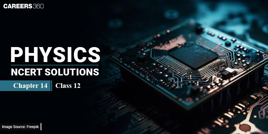
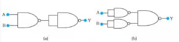
Q.8(a) You are given the two circuits as shown in Fig. Show that circuit
(a) acts as OR gate while the circuit
Answer:
Here, THE Input = A and B
Output = Y
The left part of the figure acts as a NOR and right part acts as NOT Gate.
The output of NOR gate = $\overline{A+B}$
the output of the NOR gate would be the input of NOT Gate and hence
$\mathrm{Y}=\overline{\overline{A+B}}=\mathrm{A}+\mathrm{B}$
Hence the figure functions like an OR Gate.
or compare the truth table by giving different input and observing the output
INPUTS | OUTPUT |
|---|---|
| A B | Y |
| 0 0 | 0 |
| 0 1 | 1 |
| 1 0 | 1 |
| 1 1 | 1 |
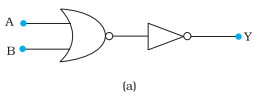
Q. 8(b) You are given the two circuits as shown in Fig. Show that circuit
Answer:
The output of NOT gate ( left part of the circuit) is the input of the NOR gate
Hence the output of total circuit Y = $\over(\overline A + \overline B)$
= $\overline{\overline A}.\overline{\overline B}$ $\overline{A+B}=\overline A. \overline B$
= $A*B$
Hence the circuit functions as AND gate.
or give the inputs 00,01,10,11 and observe the truth table
INPUTS | OUTPUT |
|---|---|
| A B | Y |
| 0 0 | 0 |
| 0 1 | 0 |
| 1 0 | 0 |
| 1 1 | 1 |
The truth table is the same as that of AND gate
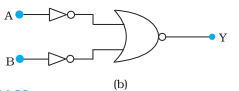
Q.9 Write the truth table for a NAND gate connected as given in the figure.
Hence identify the exact logic operation carried out by this circuit.
Answer:
Here A is both input of the NAND gate and hence Output Y will be
$Y = \overline {A*A}$
$Y = \overline {A} + \overline A$
$Y = \overline {A}$
Hence circuit functions as a NOT gate.
The truth table for the given figure:
| Input | Output |
| A | Y |
| 0 | 1 |
| 1 | 0 |
Answer:
a)
A and B are inputs of a NAND gate and output of this gate is the input of another NAND gate so,
Y = $\over(\overline {A.B})(\overline {A.B})$
Y= $\over(\overline {A.B})$ $+$ $\over(\overline {A.B})$
Y= $AB$
Hence this circuit functions as AND gate.
b)
A is input to the NAND gate output of whose goes to the rightmost NAND gate. Also, B is input to the NAND gate whose output goes to the rightmost NAND gate.
Y = $\over \overline A .\overline B$
Y = $\over\overline A .$ + $\over\overline B.$
Y = A + B
Hence the circuit functions as an OR gate .
Alternative method
fig. a
construct the truth table by giving various input and observe the output
| INPUT | INTERMEDIATE OUTPUT | OUTPUT |
| 00 | 1 | 0 |
| 01 | 1 | 0 |
| 10 | 1 | 0 |
| 11 | 0 | 1 |
The above truth table is the same as that of an AND gate
fig. b
| INPUTS | OUTPUT |
| 00 | 0 |
| 01 | 1 |
| 10 | 1 |
| 11 | 1 |
The above truth table is the same as that of an OR gate
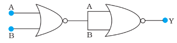
(Hint: $A=0,B=1$ then $A$ and $B$ inputs of second NOR gate will be $0$ and hence $Y=1.$ Similarly work out the values of $Y$ for other combinations of $A$ and $B.$ Compare with the truth table of OR, AND, NOT gates and find the correct one.)
Answer:
A and B are the input od a NOR gate and Output of this NOR gate is the Input of Another NOR gate whose Output is Y. Hence,
Y = $\over(\overline{A+B} + \overline{A+B})$
Y = $\over\overline {A+B}$ . $\over\overline {A+B}$
Y = A + B
Hence Circuit behaves as OR gate.
Truth table
| INPUTS | OUTPUT |
| 00 | 0 |
| 01 | 1 |
| 10 | 1 |
| 11 | 1 |
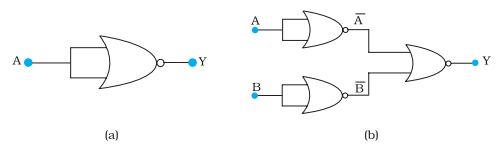
Answer:
a)
A is the two input of the NOR gate and Hence Output Y is:
Y = $\overline {A+A}$
Y = $\overline {A}$
Hence circuit functions as a NOT gate.
TRUTH TABLE:
| INPUT | OUTPUT |
| 0 | 1 |
| 1 | 0 |
b) A is the two input of a NOR gate whose output(which is $\overline {A}$ ) is the one input of another NOR gate. B is the two input of NOR gate whose output (which is $\overline {B}$ ) is the input of another NOR gate. Hence,
Y = $\over\overline {A} + \overline {B}$
Y = $\over\overline {A}$ . $\over\overline {B}$
Y = A.B
Hence it functions as AND gate.
TRUTH TABLE:
| INPUTS | OUTPUT |
| 00 | 0 |
| 01 | 0 |
| 10 | 0 |
| 11 | 1 |
Class 11 physics NCERT Chapter 12: Higher Order Thinking Skills (HOTS) Questions
Q1:
For an amplifier (NPN), VBC = 0, $\beta=50$, IC = 2.475 mA. Then the value of IB = ?
Answer:
As we learn
Relation between emitter current, Base current, collector current -
$
I_E=I_B+I_C
$
- wherein
$I_E=$ Emitter Current
$I_B=$ Base Current
$I_C=$ Collector Current
$
I_B=\frac{I_C}{\beta}=\frac{2.475}{50}=49.5 \mathrm{~mA}
$
Q2:
A Si diode has a saturation current of 10-7 A. Calculate the junction current for a forward bias of 0.7 V and 300 k (y = 2 for Si and V = 26 mV)
Answer:
As we learn,
Relation between current I & Voltage V -
$I=I_0\left(e^{\frac{c v}{K T}}-1\right)$
- wherein
K = Boltzmann constant
I0 = reverse saturation current
In forward bias
$e^{\frac{r v}{K T}}>>1$
Then, the forward biasing current is
$I=I_0 \cdot e^{\frac{c v}{K T}}$
$I=I_0\left(e^{\frac{\mathrm{cv}}{K T}}-1\right)=I_0\left(e^{\frac{v}{y+V_T}}-1\right)=10^{-7}\left(\frac{0.7}{2 \times 26}-1\right)=70 \mathrm{~mA}$
Q3:
Find the current through the circuit for Si diode`

Given that -
Knee voltage for Ge is 0.3 V
Knee voltage for Si is 0.7 V
Answer:
Knee voltage of P-N junction -
It is defined as that forward voltage at which the current through the junction starts rising rapidly with increase in voltage .
Knee voltage for Ge is 0.3 V
Knee voltage for Si is 0.7 V
$I=\frac{3.4-0.7}{600}=\frac{2.7}{600}=4.5 \mathrm{~mA}$
Q4:

The truth table for the above logic circuit is the same as that of :
Answer:
As we learn
NOR Gate -
NOT + OR Gate

- wherein
$Y=\overline{A+B}$
A and B are input
Y is output

The output (y) of two input (A, B) NOR gates is :
$Y=\overline{A+B}$
Q5:
For the circuit shown current through 1.5K$\Omega$ is:

Answer:
As we learn
Zener diode can operate continuously without being damaged in the region of reverse bias
- wherein
1) It acts as a voltage regulator
2) In forward biasing it acts as an ordinary diode.
$I_L=\frac{V_Z}{1.5 \mathrm{~K}}=\frac{6}{1.5 \times 10^3}=4 \mathrm{~mA}$
CBSE Class 12th Syllabus: Subjects & Chapters
Select your preferred subject to view the chapters
Semiconductor Electronics: Materials, Devices and Simple Circuits Class 12 Chapter 14: Topics
-
Classification Of Metals, Conductors And Semiconductors
-
Intrinsic Semiconductor
-
Extrinsic Semiconductor
-
P-N Junction
-
Semiconductor Diode
-
Application Of Junction Diode As A Rectifier
Semiconductor Electronics: Materials, Devices and Simple Circuits Class 12 Chapter 14: Notes
Metals, Conductors & Semiconductors
Why do some materials light up your circuits while others block the buzz? Metals conduct electricity well. Conductors let current pass easily. Semiconductors—like silicon—are in-between, and insulators stop the flow completely.
Intrinsic Semiconductor
Pure semiconductors like silicon have equal electrons and holes. They don’t conduct much—until heat gets them moving!
Extrinsic Semiconductor
- Add a pinch of impurity, and things change!
- n-type: Extra electrons (via elements like phosphorus).
- p-type: Extra holes (via elements like boron).
- Doping boosts conductivity.
JEE Main Highest Scoring Chapters & Topics
Just Study 40% Syllabus and Score upto 100%
Download EBookP-N Junction
A magical meeting of p-type and n-type. It only lets current flow one way—thanks to the mysterious depletion region!
Semiconductor Diode
A p-n junction in action. It’s a one-way gate for current—perfect for letting power flow forward and blocking the backflow.
Junction Diode as Rectifier
- Want to turn AC into DC? Diodes do the trick!
- Half-wave: Uses one side of AC.
- Full-wave: Uses both sides.
- It’s how your gadgets get steady power.
Approach to Solve Questions of Semiconductor Electronics: Materials, Devices and Simple Circuits
- Master the basic fundamentals of semiconductors.
- Know what conductors, insulators, and semiconductors are.
- There are two categories of semiconductors: intrinsic (pure) and extrinsic (doped).
- Know the types of doping
- n-type: Introduction of pentavalent impurity → Additional electrons
- p-type: Introduction of trivalent impurity → Increased holes
- Learn important parts:
- Diode: Recognize forward and reverse bias.
- Zener diode: Used for voltage control
- Transistors (n-p-n, p-n-p): Current amplification and switching
- Learn circuit behavior
- Explain how voltage and current act in forward/reverse-biased diodes
- Study rectifier circuits: Half-wave and full-wave.
- Apply proper formulas-
-
Current gain in a transistor: $\beta=\frac{I_C}{I_B}$
-
$
\left.I_E=I_B+I_C \text { (Emitter current }=\text { Base }+ \text { Collector }\right)
$
- Study I-V characteristics- Draw and label graphs for diodes and transistors.
- Learn logic gates (brief introduction)- AND, OR, NOT (if included) – Know the truth tables and how they apply.
- Practice circuit numericals- Recognize biasing, compute currents, and perceive role of power supply
- Know applications-
- Diodes: Rectification, switching
- Transistors: Logic circuits, amplifiers
- Study the theory and practice NCERT questions- Most questions are questions about numbers or ideas, so put both.
What Extra Should Students Study Beyond NCERT for JEE/NEET?
NCERT solutions for class 12 physics chapter-wise
Also Check NCERT Books and NCERT Syllabus here:
- NCERT Books Class 12 Physics
- NCERT Syllabus Class 12 Physics
- NCERT Books Class 12
- NCERT Syllabus Class 12
NCERT solutions subject wise
Frequently Asked Questions (FAQs)
Q: Why are NCERT Solutions Class 12 Physics necessary to students?
A:
They give step-by-step explanations to make the not-so-easy concepts easier and to solve questions in exercises in a straightforward manner.
Q: Are NCERT Solutions sufficient in achieving good marks in Class 12 board exams?
A:
Yes, NCERT Solutions is enough to pass boards yet however having practice and doing sample papers will increase your mark.
Q: Are these NCERT Solutions useful in JEE and NEET preparation?
A:
Absolutely! Most of the questions in JEE and NEET are directly and indirectly linked to the NCERT concepts; hence, these solutions assist in building a great foundation.
Q: Is it possible to download NCERT Solutions of Class 12 Physics chapter-wise in PDF?
A:
Yes, all NCERT Solutions in each Chapter can be downloaded as PDFs to study and revise.
Q: What is the best way to use NCERT Solutions Class 12 Physics?
A:
You should read the NCERT textbook, go over the NCERT Solutions to clear any confusion, then do previous year papers and mock tests.
Articles
Related Stories
|
Upcoming School Exams

Certifications By Top Providers
Explore Top Universities Across Globe
Questions related to CBSE Class 12th
On Question asked by student community
Have a question related to CBSE Class 12th ?
Hello,
Since you have passed 10th and 12th from Delhi and your residency is Delhi, but your domicile is UP, here’s how NEET counselling works:
1. Counselling Eligibility: For UP NEET counselling, your UP domicile makes you eligible, regardless of where your schooling was. You can participate in UP state
Hello,
You can access Free CBSE Mock tests from Careers360 app or website. You can get the mock test from this link : CBSE Class 12th Free Mock Tests
Hope it helps !
Yes, it is possible for a student who has done their 12th grade already to take upto 4 exams of their requirement. This is possible through the NIOS, NATIONAL INSTITUTE OF OPEN SCHOOLING. Get more info about the exam and the board through the following link.
For CBSE the PREVIOUS YEARS PAPERS can be accessed through the following link for the Concerned subjec by careers360.
Consequently Careers360 does also have a chapter wise scheme of PYQs, you can access the STUDY MATERIAL (PYQs.) from the following link -
https://school.careers360.com/boards/cbse/cbse-question-bank
Thankyou.
Hello,
Sorry, but JoSAA does not accept marks from two different boards for the same qualification during counselling. However, you can use your NIOS marks to meet the JEE Main/Advanced eligibility criteria if they are better than your CBSE marks. You can use your NIOS marks for the eligibility check,
Colleges After 12th
Applications for Admissions are open.
This ebook serves as a valuable study guide for NEET 2025 exam.
NEET Previous 10 Year Questions
Get nowThis e-book offers NEET PYQ and serves as an indispensable NEET study material.
JEE Main Important Physics formulas
Get nowAs per latest syllabus. Physics formulas, equations, & laws of class 11 & 12th chapters
JEE Main Important Chemistry formulas
Get nowAs per latest syllabus. Chemistry formulas, equations, & laws of class 11 & 12th chapters
JEE Main high scoring chapters and topics
Get nowAs per latest 2024 syllabus. Study 40% syllabus and score upto 100% marks in JEE
JEE Main Important Mathematics Formulas
Get nowAs per latest syllabus. Maths formulas, equations, & theorems of class 11 & 12th chapters
CBSE Class 12th Notifications
Never miss CBSE Class 12th update
Get timely CBSE Class 12th updates directly to your inbox. Stay informed!